Micro- and nano-scale manufacturing has been the subject of research and industrial focus over the past decades. In recent years, atomic and close-to-atomic scale manufacturing (ACSM) has emerged towards realising atomic-scale precision by addressing the digital nature of matters, i.e., an integer number of discrete atomic distances and associated quantum effects. Lithography-based technology forms the basis of micro-electro-mechanical systems (MEMS) manufacturing, and ultra-high precision manufacturing technologies have also been developed to cover micro-, nano- and atomic-scale dimensions and accuracies.
These fundamentally different technologies are combined to exploit their strengths in advanced micro- nano-manufacturing process chains. An example can be found in the use of lithography-based technologies to establish nanostructures subsequently transferred to 2½D/3D geometries via micro moulding or thermal imprinting, or in micro-scale additive manufacturing processes combined with precision subtractive finishing.
Micro manufacturing processes are the key enabling technologies to bridge the gap between the nano- and the macro-worlds, and to integrate different dimensional scales into mass-manufacturing processes, while digital technologies enable data exchange for process chain integration across the different scales.
Accordingly, the Special Interest Conference on Micro/Nano Manufacturing in combination with the International Academy of Engineering and Technology Symposium on ACSM and Digital Manufacturing (AET) will focus on novel methodological developments in micro-, nano-, atomic-scale and digital manufacturing, i.e., on novel process chains including process optimisation, quality assurance approaches, metrology, process chain integration. The workshop will host keynotes and several presentations and posters covering the latest developments and research on these increasingly important topics. The conference will also host a training seminar covering aspects of micro/nano manufacturing in practice.
Themes :
| ·Micro-Nano & Atomic-Scale Manufacturing Technologies & Applications | ·Ultraprecision Machining Technologies at the Micro/Nano/Close-to-Atomic Scales | ·Metrology & Quality Control for Micro Parts and Nano/Close-to-Atomic Features |
| ·Precision Replication, Additive Techniques, Process Chain Integration | ·Assembly & Handling in the Micro and Nano regimes | ·Digital Technologies for Precision Manufacturing |
The local hosts and organising committee supporting euspen for this Special Interest Conference meeting on Micro/Nano Manufacturing & AET are: Prof. Dr Thomas Arnold from Leibniz Institute of Surface Engineering (IOM), DE; Dr Denis Dontsov from SIOS Meßtechnik GmbH, DE; Dr Oltmann Riemer from LFM (Bremen), DE; Prof. Dr Stefan Sinzinger from Technische Universität Ilmenau, DE; Associate Prof. Guido Tosello from Technical University of Denmark; Dr. Xichun Luo from University of Strathclyde, Glasgow; and Prof. Nabil Anwer from the Paris-Saclay University, FR.
The Micro/Nano Manufacturing meeting chair is Prof. Nabil Anwer
This event is supported by our local hosts:
Key Dates
1st May 2025 : Delegate Registration Opens
12th May 2025 : Online abstract submission deadline
20th May 2025 : Notification of presentation acceptance (oral/poster)
Registration Fees
*Student members fee is not inclusive of the networking dinner.
All speakers and presenters must register for the conference using the appropriate delegate fee.
Registration
The euspen SIC meeting on Micro/Nano Manufacturing & AET complies with international VAT/IVA/VAT MOSS rules and as such the relevant Standard VAT of France VAT 20% will be applied to all delegate registration invoices. Please select the appropriate payment option below.
Select Credit Card if you would like to pay by credit card :-
Select Invoice if you would like to pay by invoice :-
- A valid Purchase Order (PO) number is required to guarantee payment.
- An administration fee of €30 will be applied.
- All invoices must be settled prior to attendance of the event. If the invoice remains outstanding at the point of attendance, the delegate will be required to pay the invoice via credit card before admittance.
- Your completed form should be sent to info@euspen.eu and an invoice will be sent to you manually.
THIS OPTION IS NO LONGER AVAILABLE. PLEASE USE THE CREDIT CARD OPTION FOR REGISTRATION AND PAYMENT. THANKYOU.
Exhibitor Information
If you would like to exhibit at this meeting, your registration fee would include:
- 1 x table (actual size to be confirmed)
- 2 x chairs
- Space for 2 roll-up banners
- 5 minute industry presentation within the programme. We would request this is not a sales pitch but more related to organisational information and real-life applications of products etc.
- 1 x delegate registration (includes the networking dinner and access to presentations)
Exhibitors
Submissions (short abstract and 4-page paper)
We are delighted to bring together leading expertise globally to an open forum for
focused presentations and discussions on Micro/Nano Manufacturing
Announcement & Call for Abstracts
Come and join your international peers and maintain a leading edge on technology, customers, partners and suppliers. Access the greatest minds in Micro and Nano research and development. Share knowledge and information and stimulate debates.
Themes
- Micro-Nano & Atomic-Scale Manufacturing Technologies & Applications
- Precision Replication, Additive Techniques, Process Chain Integration
- Ultraprecision Machining Technologies at the Micro/Nano/Close-to-Atomic Scales
- Assembly & Handling in the Micro and Nano regimes
- Metrology & Quality Control for Micro Parts and Nano/Close-to-Atomic Features
- Digital manufacturing
Submission of abstracts
Abstracts are expected to describe original work, previously unpublished and should indicate new and significant advances and their importance. Initially short abstracts comprising of approx. 300 words in length should be submitted online using the below links.
Following review a review of submitted abstracts, authors will be notified of acceptance of presentation mode (poster/oral) no later than 20th May 2025 .
The invitation to submit an abstract does not constitute an offer to pay travel, accommodation or registration costs associated with the conference. Similarly, no speaker fee is paid to successful participants. All speakers must register for the conference and transfer registration fee. In specific cases the organising committee reserves the right to deviate from the standard procedure.
Submission deadline: 12th May 2025
Keynotes
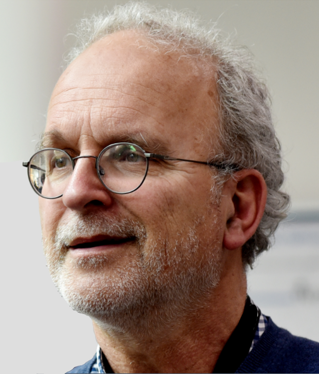
Professor Dr Fred Roozeboom
University of Twente, Netherlands
Current Status and Future Outlook in Atomic-Scale Processing
The IRDS-2022 Roadmap catches the three different scaling ages for the past and upcoming decades. Today, we witness the transition to the third age named ‘3D Power Scaling’ in a sequence of eras that started with straightforward geometrical scaling by continuous shortening of the wavelengths (from regular UV to deep UV/immersion) used in lithographic patterning of planar transistor structure. In the second ‘equivalent scaling’ era, new superior material properties and critical dimensions nearing single-digit nanometer values could still be realized by cost-effective technology solutions.
Ever more complex device architectures requiring extreme edge placement accuracy, layer conformality and shape fidelity in all processing steps (deposition, etching, cleaning) can only be realized by Atomic Layer Deposition (ALD) and Atomic Layer Etching (ALE). Today, these techniques are indispensable in the manufacture of fully 3D-integrated devices using vertical intra- and inter-chip concepts, thus alleviating the need for capital-intensive EUV-tools, at ~40% total tool costs for modern fabs.
This keynote focuses on the fundamentals and latest trends in Atomic Layer Processing in sub-10 nm fabrication of 3D-architectures. ALD and ALE have manifested to cost-effectively bridge the >10-years incubation time needed to bring EUV-technology from prototype to commercial use. These techniques can be uniquely used to create 3D-devices in dedicated isotropic (thermal and radical-enhanced) and anisotropic (directional and ion-enhanced) processing modes. Here, energetic species (radicals and/or ions in a plasma) are used in one or two steps, with ions yielding anisotropic profiles (used in FinFET logic and 3D-NAND memory), and neutrals/radicals yielding isotropic profiles to create single-digit-nm features in devices containing horizontal nanowires, nanosheets and ‘forksheets’ in GAA-FETs, and complementary FETs.
Biography
Fred Roozeboom holds a doctorate in technical sciences from University of Twente (Netherlands) with specialization in inorganic chemistry and catalysis. After three years in catalysis at ExxonMobil R&D Labs in Baton Rouge (USA), he joined Philips Research (from 2007: NXP) in Eindhoven, Netherlands to work most of his life on thin-film technology and plasma processing (1983-2009). From 1997-2009 he led a team that focused here on applications in 3D passive and heterogeneous integration for System-in-Package devices for wireless communication and power management. In 2007 he became Research Fellow and also full professor at TU Eindhoven (2007-2021), working on atomic layer deposition and etching. In 2009 he left NXP to join TNO Holst Centre to work on spatial atomic layer process and reactor design.
In 2021 he left TU Eindhoven and TNO to join University of Twente as guest (emeritus) professor, where his research focuses on inorganic membranes for nanofiltration applications. Since 2021 he is or was also consultant for high-tech industry in applications of thin-film processing in EUV optics lifetime, 3D Li-ion batteries, etching and greenhouse gas emission reduction.
Fred holds over 50 US patents, granted or pending, and published 200+ papers in journals (h-index 44 Scopus). He is ECS Fellow and AVS Fellow, and the winner of the ECS 2023 Gordon E, Moore Medal Award.

Professor Seeram Ramakrishna
National University of Singapore, Singapore
Electrospinning of Intelligent and Sustainable Materials
Historical observations suggest that humans are increasingly living in a manufactured world. Expectations on the materials for future manufactured products include new functionalities, intelligence and sustainability in addition to the usual performance, availability, and cost criteria.
Intelligent material interacts reversibly with its environment, or responds or adapts to changes in the environment. Two types of intelligent materials are envisaged: a) assisted intelligent materials rely on externalities and b) built-in intelligent materials are fully self-sufficient.
Sustainable material fosters a healthy living ecology via the elimination or reduction of associated greenhouse gas (GHG) emissions, wastage, and resources depletion. They are purposely designed or selected with lower ecological footprint and human health effects, and higher circularity and regenerative potential.
In recent years, electrospinning emerged as a nanotechnology method of manufacturing science and engineering. This seminar illustrates this technology with strategies for producing sustainable and intelligent materials | products.
Biography
Academician Seeram Ramakrishna is a world-renowned professor at the National University of Singapore (NUS). He is a recipient of the China Government Friendship Award and Chang Jiang Scholar of Ministry of Education, China. He is among the top four scientists of Singapore (https://ddec1-0-en-ctp.trendmicro.com:443/wis/clicktime/v1/query?url=https%3a%2f%2ftop2percentscientists.com%2ftop%2d10%2dscientists%2din%2dsingapore%2d2024%2f&umid=66178215-62d6-4b22-93be-a789d6ce54e9&rct=1755841293&auth=8d3ccd473d52f326e51c0f75cb32c9541898e5d5-aeb640c0541148a57b1718ad88942d9f80b4d28a).
He is named among the World’s Most Influential Minds (Thomson Reuters) and a Highly Ranked Scholar (Scholar GPS) with more than 500 Q1 journals papers with 217 H-Index and about 220,126 citations. His contributions also appeared in journals such Nature, Nature Reviews Methods, Nature Communications, Matter, so on. Highest professional distinctions include Fellow | Foreign Academician of Chinese Academy of Engineering; UK Royal Academy of Engineering (FREng); Singapore Academy of Engineering; Indian National Academy of Engineering; ASEAN Academy of Engineering & Technology; International Academy of Engineering and Technology; and International Academy of Bionic Science. He is also an elected Fellow of AAAS, ASM International, ASME, AIMBE, USA; IMechE and IoM3, UK; ISTE, India; and IUBSE (FBSE). Besides, he is also a Senior Chartered Engineer (Sustainability) of the Institution of Engineers Singapore in 2025. He received a PhD from the University of Cambridge, UK, and TGMP from Harvard University, USA.
He received advanced research experiences from MIT and Johns Hopkins University, USA and KIT, Japan. He is a Chair Professor of Tsinghua University and Xinghua Distinguished Chair Professor, China; Distinguished Professor of IIT Hyderabad, India; Everest Chair of MBUST, Nepal, and Vice-Chairman of World Artificial Consciousness Association (WACA). Out of three decades of working at the National University of Singapore (NUS), about 15 years of senior academic leadership includes NUS Vice-President (Research Strategy); Dean of NUS Faculty of Engineering; Director of NUS Enterprise; Director of NUS Industry and Technology Relations Office (INTRO); Director of NUS International Relations Office (IRO); Chairman of Solar Energy Institute of Singapore (SERIS); Director of NUS Bioengineering Initiative; and Director of NUS Nanoscience & Nanotechnology Initiative (NUSNNI).
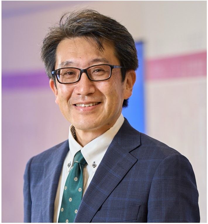
Professor Kazuya Yamamura
Research Center for Precision Engineering, Graduate School of Engineering, The University of Osaka, Japan
Achieving atomically smooth diamond substrates by plasma-assisted polishing
Diamond has the highest hardness and thermal conductivity among any substance, so it is used in tools for cutting and grinding, X-ray window materials, heat spreader materials, and so on. Recently, due to its excellent electronic properties, it has been expected to be used as a material for quantum devices and power devices. However, diamond is extremely difficult to polish due to its hardness and chemical inertness. In conventional diamond polishing, the scaife polishing using diamond abrasive causes cracks and subsurface damage to the substrate, and in the case of CMP, the material removal rate is very low.
By applying plasma-assisted polishing to the polishing of diamond substrates, we have succeeded in obtaining atomic order surface roughness with high efficiency and without introducing subsurface damage. In this presentation, the characteristics of plasma-assisted polishing for single crystal and polycrystalline diamond substrates will be introduced.
Biography
Dr. Yamamura is a Distinguished Professor at the University of Osaka and Director of the Center for Precision Engineering at the Graduate School of Engineering. And he is an associate member of CIRP and a fellow of the Japan society for Precision Engineering (JSPE). His research area is development of physicochemical ultraprecision nanomanufacturing method and its application. By using numerically controlled plasma vaporization machining, he succeeded in uniforming the thickness distribution of quartz wafers to less than 2 nm, and contributed to the development of a process for mass-production of the world’s smallest quartz crystal units. Furthermore, he invented the plasma-assisted polishing technology, which has succeeded in finishing of difficult-to-polish materials such as GaN and diamond substrates with high efficiency and damage-free.
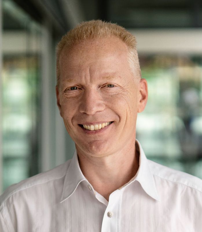
Professor Dr. U.D. Zeitner
Senior Director, Opto-Mechanical Systems, Fraunhofer IOF
Advanced fabrication technologies for scaling optical micro- and nano-structures to application relevant areas
In modern photonics the use of nano-structures offer the access to a wide range of novel functionalities not realizable with conventional optical components. Popular examples of such structures are the so called optical meta-materials which utilize sub-wavelength sized metallic or dielectric nano-structures for the flexible manipulation of amplitude and phase of an optical field. Such structures have their own challenging requirements on the nano-fabrication techniques. The patterns are often curvilinear, require a precise shape control, need to be placed with very high positioning accuracy over large distances spreading several tenths of centimeters, and need to be transferred into various materials with high aspect ratio.
The availability of high-resolution and high throughput lithographic fabrication technologies such as electron-beam lithography based on Variable Shaped Beam writing and Character Projection – in combination with complementary technologies such as e.g. Atomic-Layer-Deposition – opens the way for the flexible use of various optical nano-structures for some of the most demanding applications. The presentation will discuss the technical features, advantages, and limitations of lithographic pattering approaches and will show how they can favorably be combined to realize optical micro- and nano-structures for applications which are as diverse as gratings for ultra-short laser pulses or high resolution spectrometers, computer generated holograms for asphere testing, optical meta-lenses, or ultra-low loss photonic integrated circuits.
Biography
Uwe D. Zeitner received his PhD in physics in 1999 for a work on diffractive optics in laser resonators from the Friedrich-Schiller-University Jena. In 2008 he received the Habilitation from the same university for his work on spatio-temporal control of light using micro-structured optics. From November 2022 until May 2025 he held a research professorship for Technical Optics at the University of Applied Sciences in Munich. Since 1999 he is with the Fraunhofer IOF, Jena, currently being a member of the scientific board.
His field of research is the development of micro- and nano-lithographic solutions for optical applications enabled by fundamental research in various fields. He has a strong background in the development of high-performance optical components and gratings for applications like laser pulse compression or space-borne spectroscopy for several missions of the European Space Agency.

Professor Martin Booth
Optical and Photonic Engineering, Department of Engineering Science, University of Oxford, United Kingdom
Adaptive laser writing for three-dimensional precision fabrication of functional devices
Adaptive optics allows for spatial control over the phase and intensity of a laser beam, making it a powerful tool to assist ultrashort pulse laser machining. Optical aberrations caused by refraction at interfaces distort the laser focus, compromising resolution and fabrication efficiency. We show how the aberrations can be dynamically compensated using adaptive optics, such as liquid crystal spatial light modulators, for improved manufacturing of functional devices. Examples include fabrication of waveguide circuits in a range of materials, fiber based Bragg sensors for harsh environments, diamond based electronics and compact tunable liquid crystal devices.
Biography
Prof Martin Booth is chair in Optical and Photonic Engineering at the University of Oxford. His research involves the development and application of adaptive optical methods in microscopy, laser-based materials processing and biomedical imaging. In particular, his group have developed numerous implementations of adaptive optics for aberration correction in high resolution microscopes and precision laser fabrication systems. He has held Royal Academy of Engineering and EPSRC Research Fellowships and an Advanced Grant from the European Research Council. In 2014 he was awarded the International Commission for Optics Prize. He was appointed Professor of Engineering Science in 2014 and Chair in Optics and Photonics in 2023. He is a fellow of SPIE, Optica, and the Institute of Physics and serves on the board of Optica. He has over 180 publications in peer-reviewed journals, over thirty patents, and has co-founded two spin-off companies, Aurox Ltd and Opsydia Ltd.